The History of the Integrated Circuit
Integrated Circuits
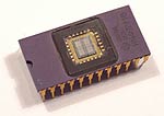
Our world is full of integrated circuits. You find several of them in computers. For example, most people have probably heard about the microprocessor. The microprocessor is an integrated circuit that processes all information in the computer. It keeps track of what keys are pressed and if the mouse has been moved. It counts numbers and runs programs, games and the operating system. Integrated circuits are also found in almost every modern electrical device such as cars, television sets, CD players, cellular phones, etc. But what is an integrated circuit and what is the history behind it?
 |
| Photo: Nobelprize.org |
Electric Circuits
The integrated circuit is nothing more than a very advanced electric circuit. An electric circuit is made from different electrical components such as transistors, resistors, capacitors and diodes, that are connected to each other in different ways. These components have different behaviors.
The transistor acts like a switch. It can turn electricity on or off, or it can amplify current. It is used for example in computers to store information, or in stereo amplifiers to make the sound signal stronger.
The resistor limits the flow of electricity and gives us the possibility to control the amount of current that is allowed to pass. Resistors are used, among other things, to control the volume in television sets or radios.
The capacitor collects electricity and releases it all in one quick burst; like for instance in cameras where a tiny battery can provide enough energy to fire the flashbulb.
The diode stops electricity under some conditions and allows it to pass only when these conditions change. This is used in, for example, photocells where a light beam that is broken triggers the diode to stop electricity from flowing through it.
These components are like the building blocks in an electrical construction kit. Depending on how the components are put together when building the circuit, everything from a burglar alarm to a computer microprocessor can be constructed.
The Transistor vs. the Vacuum Tube
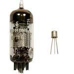
Of the components mentioned above, the transistor is the most important one for the development of modern computers. Before the transistor, engineers had to use vacuum tubes. Just as the transistor, the vacuum tube can switch electricity on or off, or amplify a current. So why was the vacuum tube replaced by the transistor? There are several reasons.
The vacuum tube looks and behaves very much like a light bulb; it generates a lot of heat and has a tendency to burn out. Also, compared to the transistor it is slow, big and bulky.
 |
 |
| The vacuum tube and the
transistor. Photo: Nobelprize.org |
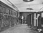
ENIAC-The first digital
computer Photo: U.S Army |
When engineers tried to build complex circuits using the vacuum tube, they quickly became aware of its limitations. The first digital computer ENIAC, for example, was a huge monster that weighed over thirty tons, and consumed 200 kilowatts of electrical power. It had around 18,000 vacuum tubes that constantly burned out, making it very unreliable.
When the transistor was invented in 1947 it was considered a revolution. Small, fast, reliable and effective, it quickly replaced the vacuum tube. Freed from the limitations of the vacuum tube, engineers finally could begin to realize the electrical constructions of their dreams, or could they?
The Tyranny of Numbers
With the small and effective transistor at their hands, electrical engineers of the 50s saw the possibilities of constructing far more advanced circuits than before. However, as the complexity of the circuits grew, problems started arising.
When building a circuit, it is very important that all connections are intact. If not, the electrical current will be stopped on its way through the circuit, making the circuit fail. Before the integrated circuit, assembly workers had to construct circuits by hand, soldering each component in place and connecting them with metal wires. Engineers soon realized that manually assembling the vast number of tiny components needed in, for example, a computer would be impossible, especially without generating a single faulty connection.
Another problem was the size of the circuits. A complex circuit, like a computer, was dependent on speed. If the components of the computer were too large or the wires interconnecting them too long, the electric signals couldn't travel fast enough through the circuit, thus making the computer too slow to be effective.
So there was a problem of numbers. Advanced circuits contained so many components and connections that they were virtually impossible to build. This problem was known as the tyranny of numbers.
Jack Kilby's Chip - the Monolithic Idea
 |
 |
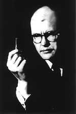
| Jack S Kilby Photo: Texas Instruments |
Kilbys first chip Photo: Texas Instruments |
In the summer of 1958 Jack Kilby at Texas Instruments found a solution to this problem. He was newly employed and had been set to work on a project to build smaller electrical circuits. However, the path that Texas Instruments had chosen for its miniaturization project didn't seem to be the right one to Kilby.
Because he was newly employed, Kilby had no vacation like the rest of the staff. Working alone in the lab, he saw an opportunity to find a solution of his own to the miniaturization problem. Kilby's idea was to make all the components and the chip out of the same block (monolith) of semiconductor material. When the rest of the workers returned from vacation, Kilby presented his new idea to his superiors. He was allowed to build a test version of his circuit. In September 1958, he had his first integrated circuit ready. It was tested and it worked perfectly!
Although the first integrated circuit was pretty crude and had some problems, the idea was groundbreaking. By making all the parts out of the same block of material and adding the metal needed to connect them as a layer on top of it, there was no more need for individual discrete components. No more wires and components had to be assembled manually. The circuits could be made smaller and the manufacturing process could be automated.
Jack Kilby is probably most famous for his invention of the integrated circuit, for which he received the Nobel Prize in Physics in the year 2000. After his success with the integrated circuit Kilby stayed with Texas Instruments and, among other things, he led the team that invented the hand-held calculator.
Robert Noyce
 |
| Robert Noyce Photo: Intel Museum Archives |
Robert Noyce came up with his own idea for the integrated circuit. He did it half a year later than Jack Kilby. Noyce's circuit solved several practical problems that Kilby's circuit had, mainly the problem of interconnecting all the components on the chip. This was done by adding the metal as a final layer and then removing some of it so that the wires needed to connect the components were formed. This made the integrated circuit more suitable for mass production. Besides being one of the early pioneers of the integrated circuit, Robert Noyce also was one of the co-founders of Intel. Intel is one of the largest manufacturers of integrated circuits in the world.
Chip Production Today - in Short
 |
| Stepping. |
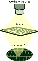
Chip production today is based on photolithography. In photolithography a high energy UV-light is shone through a mask onto a slice of silicon covered with a photosensitive film. The mask describes the parts of the chip and the UV-light will only hit the areas not covered by the mask. When the film is developed, the areas hit by light are removed. Now the chip has unprotected and protected areas forming a pattern that is the first step to the final components of the chip.
Next, the unprotected areas are processed so their electrical properties change. A new layer of material is added, and the entire process is then repeated to build the circuit, layer by layer. When all the components have been made and the circuit is complete a layer of metal is added. Just as before, a layer of photosensitive film is applied and exposed through a mask. However, this time the mask used describes the layout of the wires connecting all the parts of the chip. The film is developed and the unexposed parts are removed. Next, the metal not protected with film is removed to form the wires. Finally, the chip is tested and packaged.
When making chips today, a process called "stepping" is often used. On a big wafer of silicon the chips are made one next to the other. The silicon wafer is moved in steps under the mask and the UV-light to expose the wafer. In this way, chip after chip can be made using the same mask each time.
Below is a more sequential description of the process of making a modern integrated circuit. But let us first take a look at the special place where integrated circuits are produced - the clean room.
The Clean Room
 |
| Child facing "bunny
suit" Photo: Intel Museum Archives |
The sizes of the components on chips produced in a modern chip fabrication plant are extremely small. For a better understanding of how small they are, pick a hair from your head and cut it in half. Now look at the cross section. On this tiny area, hard to see with the bare eye, you can fit thousands of modern transistors.
With sizes this small, the production of a chip demands precision at an atomic level. Tiny particles like a hair, a speck of dust, a dead skin cell, bacteria or even the single particles in tobacco smoke become huge objects that are big enough to ruin a chip.
Therefore, chip production takes place in a clean room. This is a specially designed room, where furniture is built from special materials that don't give off particles, and where extremely effective air filters and air circulation systems change the air completely up to ten times a minute.
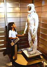
To further prevent contamination, workers wear special suits called "bunny suits." These protective outfits are made of ultra clean material and sometimes have their own air filtering systems.
Chip Production Today - in Detail
Building an integrated circuit like a computer chip is a very complex process. It is divided into two major parts, front end and back end. In the front end, you make the components of the circuit. In the back end, you add metal to connect the components and then you test and package the chip. Below is a simplified description of the steps.
Front End – Construction of the Components
 |
1. |
 |
2. From the construction plans, masks with the circuit patterns are made. |
 |
3. Under precisely monitored conditions, a pure silicon crystal is grown. Circuit manufacturing demands the use of crystals with an extremely high grade of perfection. |
 |
4. The silicon is sawed into thin wafers with a diamond saw. The wafers are then polished in a number of steps until their surface has a perfect mirror-like finish |
 |
5. The silicon wafer is covered with a layer of insulating silicon oxide. |
 |
6. A covering film of protective material is put on top of the insulating silicon oxide. This material, a bit like the film in any ordinary camera, is sensitive to light. |
 |
7. UV-light is shone through a mask and onto the chip. On the parts of the chip that are hit by light, the protective material breaks apart. |
 |
8. The wafer is developed, rinsed and baked. The development process removes the parts of the protective material exposed to light. |
 |
9. The wafer is treated with chemicals in a process called "etching." This removes the unprotected insulating material, creating a pattern of non-protected silicon wafer parts surrounded by areas protected by silicon oxide. |
 |
10. The wafer is run through a process that alters the electrical properties of the unprotected areas of the wafer. This process is called "doping." Steps 5-10 are repeated to build the integrated circuit, layer by layer. Other layers of conducting or isolating layers may also be added to make the components. |
| Back End – Adding the Connecting Wires | |
 |
11. Finally, when all the components of the chip are ready, metal is added to connect the components to each other in a process called metalization. This is done in a way similar to the making of the components. First a conducting metal like copper is deposited over the chip. |
 |
12. On top of the metal a layer of UV-sensitive photo resist is added. |
 |
13. Next, a mask that describes the desired layout of the metal wires connecting the components of the chip is used. UV-light is shone through this mask. The light hits the photo resist that isn't protected by the mask. |
 |
14. In the next step, chemicals are used to remove the photo resist hit by UV-light. |
 |
15. Another step of etching removes the metal not protected by photo resist. |
 |
16. This leaves a pattern of metal that is the same as the one described by the mask. Now, the chip has a layer of wires that connect its different components. |
 |
17. Today, most integrated circuits need more than one layer of wires. Advanced circuits may need up to five different layers of metal to form all the necessary connections. In the last picture we have added another layer of metal to our example. As you can see, a layer of insulating material is put between the two metal layers to prevent the wires from connecting in the wrong places. Of course, to add the second layer we had to go through the same steps as when adding the first layer of metal. |
 |
18. When the final layer of connecting metal wires have been added, the chips on the silicon wafer are tested to see if they perform as intended. |
 |
19. The chips on the wafer are separated with a diamond saw to form individual integrated circuits. |
 |
20. Finally, each chip is packed into the protective casing and subjected to another series of tests. The chip is now finished and ready to be shipped to manufacturers of digital devices around the world. |
The Evolution of the Integrated Circuit
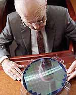
The integrated circuit has come a long way since Jack Kilby's first prototype. His idea founded a new industry and is the key element behind our computerized society. Today the most advanced circuits contain several hundred millions of components on an area no larger than a fingernail. The transistors on these chips are around 90 nm, that is 0.00009 millimeters*, which means that you could fit hundreds of these transistors inside a red blood cell.
 |
| Jack Kilby examines a wafer
filled with chips. Photo: Texas Instruments |
Each year computer chips become more powerful yet cheaper than the year before. Gordon Moore, one of the early integrated circuit pioneers and founders of Intel once said, "If the auto industry advanced as rapidly as the semiconductor industry, a Rolls Royce would get a half a million miles per gallon, and it would be cheaper to throw it away than to park it."**
*1 inch = 25.4 millimeters**1 US gallon = 3.8 litres, 1 mile = 1.6 km
First published 5 May 2003
| Related Laureate | SEE ALSO | TIPS |
in Physics 2000 - Jack S. Kilby |
Semiconductors The Transistor |
Play "Techville" - a Game About the Integrated Circuit |